VCSEL / Photodiode Chip Burn-in / Lot Acceptance Test
December 01, 2018
Burn-in or known as lot acceptance test is an electrical stress test that typically applies voltage and temperature to a device as an accelerating factor of latent reliability failure. The objective is to screen out and eliminate potential failure at the earlier stage before module level production.
Since die performance quality and reliability is critical in specific fields of application, like proximity sensing, 3D sensing and data transmission, Testar established the process of burn-in for photodiode as a first step to provide a turnkey solution to our important partners.
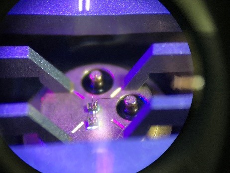
The burn-in process or lot acceptance test involves building up a sample of the die in a packaging platform that allows turning on the device in given environment and electrical testing which is beyond what can be performed on bare die. Normally, bare die can only be tested at room temperature electrically and limited testing items optically.
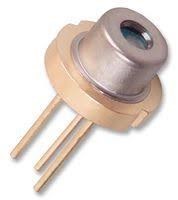
Our burn- in/ LAT includes high temperature operating life test (HTOL), wet and high temperature operating life test (WHTOL) and wire pull test (WPT). We can customize the test conditions to meet you qualification needs with ESD safety requirement. Test samples can be built in TO can package and PCB platform with in-house die bond, wire bond and capping process. As for wire bonding, currently a standard 1.0 mil gold wire is used for wire pull test following customer’s requirement or the bond wire modeling standard JEDEC / JESD59.


Once the burn-in or lot acceptance test is completed, test results will be provided as a proof of reliability and the wafer batch can be delivered to following assembly house. With the goal of an one-stop-shop service provider, the advantages of established burn-in process in Testar are easier contract manufacturing management, lower logistics cost and shortened cycle time for our customers.

