About
Test Services
Optoelectronic Testing (LED, VCSEL/Photodiode)
Chip Probing
Die sorting, Wafer Reconstruction (RECON)
Automatic Visual Inspection (AVI)
Burn-in
Semiconductor Testing
Chip Probing
IC Functional Testing
Advantage
News
Contact
Die sorting, Wafer Reconstruction (RECON)
Testar 晶測電子
Test Services
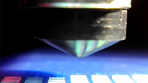
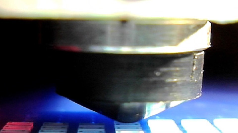
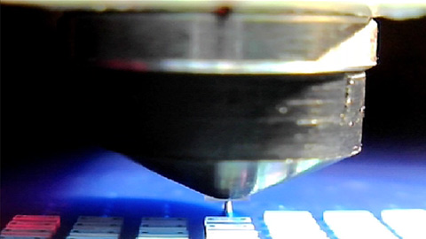
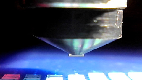
Die sorting, Wafer Reconstruction (RECON)
Key Feature
Auto alignment
Up to 12” wafer
Chip size: Up to 7000um x 7000um
Fully Automation
Real-time data management
Flexibility of output form (Metal frame, Grip ring, GEL PAK, WAFFLE PAK, etc…)
Request For Quote
+886-3-327-9600
testarservice@testar.com.tw
68,Hwa-Ya 1st Road, Hwa-Ya Technology Park, Taoyuan Hsien 333, Taiwan
333桃園市龜山區華亞科學園區華亞一路68號
Quick Links
About Testar
Test Services
Testar Advantage
Testar News
Privacy Policy
Follow us on
About
Test Services
Optoelectronic Testing (LED, VCSEL/Photodiode)
Chip Probing
Die sorting, Wafer Reconstruction (RECON)
Automatic Visual Inspection (AVI)
Burn-in
Semiconductor Testing
Chip Probing
IC Functional Testing
Advantage
News
Contact